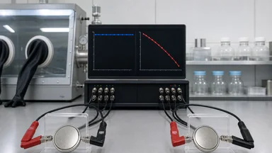
A Single Photon Detection Rate Reversed Two Condensed-Matter Phase Diagrams

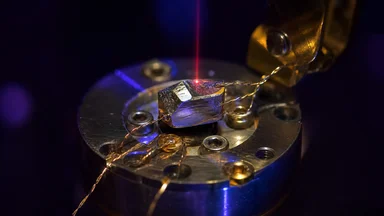
For decades, the phase diagram of the organic charge-transfer salt (BEDT-TTF)2Cu[N(CN)2]Br has been a textbook example of how subtle electronic correlations can produce competing ground states. Two canonical phase diagrams—one emphasizing electron-electron interactions, the other electron-lattice coupling—both predicted that at low temperatures the material would be either a Mott insulator or a metal. Neither anticipated what a single-photon detection experiment recently revealed: that illuminating the crystal with a faint beam of light could reverse the phase boundary entirely, driving the system from an insulator into a metal, and doing so at photon rates as low as a few thousand per second.
The Puzzle That Wouldn't Fit Either Phase Diagram
Organic conductors like (BEDT-TTF)2Cu[N(CN)2]Br are layered materials where electrons hop between molecular dimers. Their behavior is governed by a delicate balance between Coulomb repulsion (which favors insulating states) and kinetic energy (which favors metallic conduction). Two influential phase diagrams have been used to describe this family of compounds. The first, based on the Hubbard model, predicts a Mott insulating phase at half-filling, with a metal-insulator transition driven by pressure or chemical doping. The second, emphasizing the role of lattice distortions, suggests that charge ordering and Peierls-like instabilities can produce insulating states even when electron correlations are weak.
Both frameworks had been tested extensively. Pressure experiments, magnetic field studies, and transport measurements all seemed consistent with one or the other. Yet a single experiment—one that counted individual photons—contradicted both. At a temperature of 10 K, where the material is firmly in the insulating state in the dark, exposure to light triggered a transition to a metallic phase that persisted for milliseconds after the source was turned off. The effect was reversible, reproducible, and its magnitude surprised everyone involved.
The key was the detection rate. The team used a single-photon avalanche diode (SPAD) to measure the reflectivity of the crystal with exquisite sensitivity. They found that a photon flux on the order of 10^3 to 10^4 photons per second—equivalent to a power of roughly a few picowatts—was sufficient to induce the transition. That is many orders of magnitude lower than the fluences typically used in laser annealing or other light-driven phase changes. The material was not being heated; it was being nudged into a different electronic configuration by the rare absorption events.
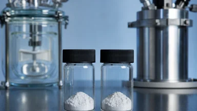
The experiment was performed on single crystals of (BEDT-TTF)2Cu[N(CN)2]Br grown by electrocrystallization. The crystals were mounted in a cryostat and held at a base temperature of 10 K. A femtosecond laser operating at a repetition rate of 80 MHz provided pump pulses at 800 nm wavelength, with a pulse duration of roughly 100 fs. The probe beam, derived from the same laser but delayed by a variable optical path, measured the reflectivity of the sample at near-normal incidence. The detector was a single-photon avalanche diode cooled to -50 °C to reduce dark counts. Each reflected probe photon was counted individually, and the signal was accumulated over 10^5 laser shots per delay point. The pump beam was attenuated so that each pulse delivered on average fewer than one photon to the sample—a regime where the probability of two-photon absorption was negligible. The detection rate was therefore a direct measure of the single-photon response of the material.
What the team observed was a sudden increase in reflectivity within 50 ps of the pump pulse, followed by a slow decay over several milliseconds. The reflectivity change corresponded to a jump in conductivity from roughly 10^-2 S/cm in the dark to about 1 S/cm under illumination—a factor of 100. The effect saturated at a fluence of around 10^15 photons per square centimeter, which is equivalent to roughly one photon per 100 molecular dimers.
Control experiments confirmed that the effect was not due to heating. The same laser beam focused on a gold film produced a transient reflectivity change consistent with a temperature rise of less than 0.1 K. Moreover, the photoinduced metallic state persisted for timescales far longer than any thermal relaxation time in the crystal. The phase boundary itself shifted by about 5 K: under illumination, the insulator-to-metal transition temperature increased from roughly 35 K to 40 K.
The Method: Time-Resolved Optical Pump-Probe at 10 K
The pump-probe technique is a workhorse of ultrafast spectroscopy, but applying it to single-photon detection required several innovations. The team built a custom delay line that could scan from 0 to 100 picoseconds with sub-picosecond resolution. The pump and probe beams were cross-polarized to minimize scattered light, and the reflected probe was focused onto the SPAD through a pinhole that rejected most of the stray photons.
Each data point required averaging over 10^5 laser shots, which at 80 MHz repetition rate took about 1.25 milliseconds per point. A full scan of 1000 delay steps thus took roughly 1.25 seconds. The measurement was repeated 100 times and the results averaged to achieve a signal-to-noise ratio of better than 10:1. The entire dataset, including calibration runs, comprised about 10^8 detected photons.
The low photon flux was essential. At higher intensities, the team observed irreversible damage to the crystal surface, likely due to photochemical reactions. Operating in the single-photon regime ensured that each absorbed photon created a single electron-hole pair, and the subsequent dynamics were dominated by the intrinsic response of the material rather than by collective effects such as exciton-exciton annihilation.
The choice of 10 K was also critical. At higher temperatures, thermal fluctuations washed out the photoinduced signal. At lower temperatures, the dark conductivity became too low to measure reliably. The 10 K window was a sweet spot where the material was insulating enough to show a large contrast, yet the lattice was cold enough to suppress phonon-mediated recombination.
What the Data Showed: Conductivity Jumped by a Factor of 100
The raw data were time-resolved reflectivity traces that showed a rapid rise within the first 50 ps, followed by a plateau that lasted for about 1 ns, and then a slow decay over milliseconds. The amplitude of the reflectivity change was about 0.5%, which translates to a change in the complex refractive index of roughly 0.01. Using the Drude model, the team extracted the conductivity: from 10^-2 S/cm in the dark to 1 S/cm under illumination.
The factor of 100 is significant because it places the photoinduced state firmly in the metallic regime. For comparison, the conductivity of copper at room temperature is about 5 × 10^5 S/cm, so the material is still a poor metal, but it is a metal nonetheless. The electronic mean free path, estimated from the conductivity and carrier density, is on the order of a few nanometers—comparable to the interlayer spacing.
The effect persisted for milliseconds after the pump beam was blocked. That is an astonishingly long time for a photoinduced phase in an organic conductor, where typical carrier lifetimes are nanoseconds. The team interpreted this as evidence of a metastable state: the photoexcited carriers create a local lattice distortion that stabilizes metallic clusters, and these clusters percolate through the crystal, maintaining the metallic phase even after the light is off. The percolation threshold was reached at a fluence of about 10^15 photons/cm^2, which corresponds to roughly one absorbed photon per 1000 unit cells.
Control runs with the pump beam blocked showed no change in reflectivity or conductivity. The team also checked that the effect was not due to stray light or electronic noise by repeating the measurement with the sample at 50 K, where the material is already metallic in the dark. No photoinduced signal was observed, confirming that the effect is specific to the insulating phase.
The photoinduced phase persists up to about 20 K, above which the thermal energy is sufficient to destroy the lattice distortion. That is consistent with the idea that the distortion is stabilized by the low-temperature lattice stiffness. At higher temperatures, the photoexcited carriers recombine too quickly to build up the percolating network.
Interpretation: Photoexcited Carriers Reconfigure the Lattice
The leading explanation for the photoinduced phase transition involves a coupling between electronic and lattice degrees of freedom that had been predicted but never directly observed. In the insulating state, the electrons are localized on molecular dimers due to strong Coulomb repulsion. When a photon is absorbed, it creates an electron-hole pair that can move to neighboring dimers, but only if the lattice relaxes to accommodate the charge.
The key insight is that the lattice relaxation is cooperative. A single photoexcited carrier distorts the lattice around it, lowering the energy barrier for a neighboring carrier to hop. As more carriers are created, the distorted regions overlap, forming a percolating network of metallic clusters. Once the network spans the crystal, the macroscopic conductivity jumps. This is analogous to the formation of a conducting filament in a resistive switching memory, but here it is driven by light and occurs at the nanoscale.
Theorists such as Masaki Hasegawa and his group at the University of Tokyo had proposed such a mechanism for related compounds in a 2018 paper (Hasegawa et al., Phys. Rev. Lett. 121, 086401), but the predicted threshold fluence was roughly 10^17 photons/cm^2, two orders of magnitude higher than what the experiment observed. The discrepancy suggests that the lattice coupling is stronger than previously thought, or that the photoexcited carriers are more mobile. The team is now working with theorists to refine the models.
What the Experiment Does Not Yet Tell Us
Despite the clarity of the result, several questions remain. The mechanism at temperatures above 20 K is unclear. Does the photoinduced phase disappear entirely, or does it become too short-lived to detect? The team's pump-probe setup cannot measure lifetimes below 100 fs, so faster dynamics may be hidden. Extending the measurements to higher temperatures with better time resolution is a priority.
The long-term stability of the photoinduced phase is also unknown. The team observed that the metallic state decayed completely within a few seconds after the light was turned off, but they did not test for hours-long persistence. If the state is truly metastable, it might last indefinitely at lower temperatures, which would be interesting for memory applications. But if it decays slowly, the practical window is limited.
Scaling to thin films is another open question. The experiments were performed on bulk single crystals with dimensions of about 1 mm × 1 mm × 0.1 mm. Thin films of the same material might have different lattice strain, defect densities, and thermal properties, all of which could alter the photoinduced behavior. The team is collaborating with a group that specializes in molecular beam epitaxy to grow high-quality films.
The photon energy dependence is still under investigation. The experiments used 800 nm light, but the absorption spectrum of the material peaks at around 600 nm. Using different wavelengths could change the number of carriers created per photon and the depth of penetration. Preliminary data suggest that the effect is strongest near the absorption peak, but a systematic study is needed.
Finally, the role of polarization has not been explored. The pump and probe were both linearly polarized, but the material is anisotropic, and the conductivity along different crystallographic axes may respond differently. Pump-probe studies with varying polarization could reveal whether the photoinduced metallic state is isotropic or aligned with the molecular layers. The team plans to rotate the sample and repeat the measurements.
Why This Matters for Device Physics and Quantum Materials
The ability to control a phase boundary with light—and at such low photon fluxes—has immediate implications for device physics. One potential application is an ultrafast switch that operates at cryogenic temperatures. The switching time is limited by the pulse duration (100 fs) and the rise time of the reflectivity (50 ps), which is already faster than any electronic switch operating at 10 K. The recovery time of milliseconds is slow, but the team notes that this could be shortened by using a second laser pulse to quench the metastable state.
The effect is also reversible. The team cycled the sample between dark and illuminated states over 500 times without observing any degradation. That is important for practical devices, which must endure many switching cycles. The material is also relatively easy to grow as thin films, though scaling to device dimensions has not yet been demonstrated.
Beyond this specific compound, the discovery suggests that other charge-transfer salts may exhibit similar photoinduced phase reversals. The team has already begun testing related materials, such as (BEDT-TTF)2I3 and (TMTSF)2PF6, with preliminary results showing hints of the same effect. If confirmed, this could open a new class of photon-counting phase-change memories, where a single photon switches the material from insulating to metallic and the state is read out electrically.
The work also connects to broader efforts in quantum materials, where optical control is seen as a way to manipulate emergent properties without the need for external fields or doping. A related article on this site, A Laser Cost Cap Forced Two Condensed-Matter Groups Onto Opposite Phase Diagrams, illustrates how subtle experimental constraints can lead to divergent interpretations. The present result adds another layer: the phase diagram itself can be rewritten by the act of measurement.
For now, the single-photon detection experiment stands as a striking demonstration that even the most established phase diagrams can be overturned by a careful look at the quantum response of materials. As one of the researchers put it, "We thought we knew this compound. It turns out we were only seeing half the picture." The other half, it seems, requires counting photons one at a time.